Seminars
Thu |
High-resolution Light Emitting Diode on Silicon (LEDoS) Micro-display and High Speed GaInAs Photodetectors on SiliconDr. Kei M. Lau, Hong Kong University of Science and Technology, Kowloon, Hong Kong | |
|
Abstract: Nitride-based visible light emitting diodes (LEDs) with high external efficiency are widely used for a variety of applications including display backlights and general lighting. The versatility of LED devices can be further enhanced by introducing individually addressable emissive elements on a silicon-based substrate with the use of flip-chip technology. Such passive matrix LED micro-arrays have been demonstrated in the past. However, the array dimensions and pixel brightness in conventional passive addressable LED arrays are limited by the loading effect in the same row or column. Recently, we employed active matrix (AM) addressing scheme to improve the operating effectiveness of LED arrays. LED on Silicon (LEDoS) display panels have great potential on applications such as micro-display in mobile electronics, portable micro-projectors, bio-sensor arrays and programmable lighting sources.
In this work, we report the development of high-resolution LEDoS micro-array display panels (6mm×7mm in size), by integrating an InGaN Multiple Quantum Well (MQW) Ultraviolent (UV) LED micro-array to a AM silicon-based substrate. The LEDoS device included two main parts: LED micro-array and AM substrate. LED micro-array and AM substrate were integrated together using flip-chip technology. When applied proper scan signal and data signal, the LEDoS display panel was programmed row by row and column by column. The LEDoS display panel generates representative micro-display images at a fresh frequency of 200 Hz, demonstrating sufficient driving capability and individually control ability.
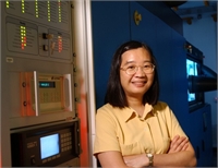
Our recent work on high-speed normal-incidence and butt-coupled p-i-n InGaAs photodetectors epitaxially grown on silicon substrates by MOCVD will also be reported. Biography: Professor Kei May Lau received the B.S. and M.S. degrees in physics from the University of Minnesota, Minneapolis, and the Ph.D. degree in Electrical Engineering from Rice University, Houston, Texas. She worked on epitaxial growth of GaAs for microwave devices at M/A-COM Gallium Arsenide Products, Inc. for two years, before joining the faculty of Electrical and Computer Engineering Department at the University of Massachusetts/Amherst. Prof. Lau initiated MOCVD, compound semiconductor materials and devices programs at UMass. Her research group conducted research on heterostructures, quantum wells, strained-layers, III-V selective epitaxy, high frequency and photonic devices. Professor Lau spent her first sabbatical leave in 1989 at the MIT Lincoln Laboratory and worked with the Electro-optical Devices Group. She developed acoustic sensors at the DuPont Central Research and Development Laboratory in Wilmington, Delaware during her second sabbatical leave ('95-'96). Since the fall of 2000, she has been with the Electronic and Computer Engineering Department at the Hong Kong University of Science and Technology (HKUST). She established the Photonics Technology Center for R&D effort in III-V materials, optoelectronic, high power, and high-speed devices. Professor Lau is a Fellow of the IEEE, and a recipient of the National Science Foundation (NSF) Faculty Awards for Women (FAW) Scientists and Engineers (1991) and Croucher Senior Research Fellowship (2008). She served on the IEEE Electron Devices Society Administrative Committee and was an Editor of the IEEE Transactions on Electron Devices (1996-2002). She also serves on the Electronic Materials Committee, and was an Editor of the Journal of Crystal Growth. Location: MIT Lincoln Laboratory |
